Building a 16-bit CPU on an Arty Z7-20
- rehsd
- Jun 24, 2022
- 6 min read
Updated: Jul 15, 2022
I am hoping to learn more about processors by building a 16-bit processor. I previously built an 8-bit processor based on Ben Eater's video series. My goal is to develop a 16-bit version of this, with a little flavor from a 65816 processor. For me, this is a huge task, and I have so much to learn. To help me think through and test some of the key aspects of a 16-bit processor design, I am going to start by implementing a 16-bit processor on an Arty Z7-20 FPGA. I have previously implemented an 8-bit processor on an Arty A7-100 FPGA.
Related posts: 16-Bit Processor (Approach to Bus and Modules) & Building an Assembler for My 16-bit Processor.
This post will be a running post, with updates as I progress through the FPGA portion of my project.
Step 1a: HDMI Output on Arty Z7
I will need a way to visualize the processor's current state, such as values of registers, counters, bus, output, etc. I am going to use the HDMI output of the Z7 to do this. While higher resolutions are easily supported, I plan to drive the video output at 640x480. If I run out of screen space, I can increase the resolution.
Steps to get to the output in the video above:
I started with the Digilent Arty-Z7-20 HDMI Out demo project. The posted project (at the time of this writing) was targeted towards Vivado/Vitis 2018.2. I used 2022.1 without any issues. Vivado will prompt to update outdated IP; I did the IP updates.
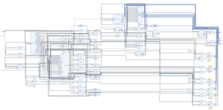
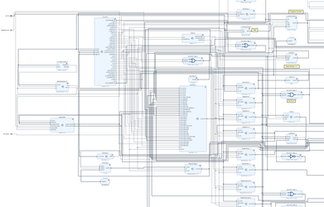
In the Vivado block design, I updated the AXI-4 Stream Subset Converter to remap the order of the bytes, so that I can use R G B (in that byte order) in Vitis. I changed TDATA Remap String to tdata[7:0],tdata[23:16],tdata[15:8]. This was done purely as a personal preference.
I don't believe I made any other notable changes in the Vivado block design.
In Vitis, I modified the demo project code by removing the unnecessary sections (e.g., demo screens). Notable changes:
I updated the MAX_FRAME and STRIDE definitions for 640x480.
MAX_FRAME: 640*480*3
STRIDE: 640*3
Added functions to support basic rendering of text and bar graphs
void PrintChar(char c, u16 start_x, u16 start_y, u8 frameNumber);
void PrintString(char chars[], u16 numChars, u16 start_x, u16 start_y, u8 frameNumber);
void DrawRectangle(u16 start_x, u16 start_y, u16 width, u16 height, u8 red, u8 green, u8 blue, u8 frameNumber);
void FillScreen(u8 red, u8 green, u8 blue, u8 frameNumber);
void DrawBarGraph8(u16 start_x, u16 start_y, u8 invertDemo, char label[], u16 labelLength, u8 frameNumber);
void DrawBarGraph16(u16 start_x, u16 start_y, u8 invertDemo, char label[], u16 labelLength, u8 frameNumber, u8 colorNumber);
void DrawClock(u16 start_x, u16 start_y, u8 invertDemo, char label[], u16 labelLength, u8 frameNumber, u8 colorNumber)
For the above functions, I write to a non-visible frame. Once the frame has been populated, I swap active frames, moving it to the active, visible frame. This has resulted in quick screen draws. For example, the top bar graph and the bottom bar graph are in sync with each other.
Step 1b: VHDL Clock Running and Being Displayed in (Updated) Debug Output
Displaying processor clock (VHDL) in HDMI output. Updated HDMI output to include hex and decimal values (in addition to the existing bar graphs). Rotary encoder allows changing the speed of the clock. A switch on the encoder enables manual clock mode, and the encoder push button pulses the clock.
Step 2: VHDL Processor Running An 8-bit Program
I now have Ben Eater's sample program of 28+14 running on the FPGA-based processor. I added debug output for the current instruction. I also added support to reset the processor via a button on the Arty Z7.
Step 3: Upgrade Processor to 16-bit
I now have Ben Eater's 8-bit processor running on my FPGA, fully upgraded to 16-bit. In the following video, the processor is adding two 16-bit numbers.
Step 4: Incremental Updates
I have been working on updating the VHDL 16-bit processor.
I am switching all opcodes to align with those from the 65816. For example, Ben used 0x05 for load immediate (LDI); I have changed this to 0x00A9 (LDA Immediate). I have changed 0x0F (HLT) to 0x00DB (STP).
I have separated the opcode and associated data (e.g., value or address) into two separate double-byte entries in ROM/RAM. Ben used a single byte, with the upper four bits for the opcode and the lower four bits for the associated data. Below is an example of assembly code and the associated output for ROM.
Assembly Code
LDA #$8E39
STP
Assembler Output
00A98E3900DBA couple of things about my approach so far.
You may have noticed that I am using big endian for byte order. I do not yet know if I will stick with big endian or switch to little endian.
Opcodes and data are stored as double-byte ROM/RAM entries. With this, I can support 65,536 opcodes. Of course, I likely will not surpass 100 opcodes. This is not the most efficient for storage, but it simplifies my design (so far, at least).
I plan to build a simple assembler to allow me to convert assembly code into assember output specific for my 16-bit processor.
Renamed the B register (used by Ben) to X and added a Y register.
I expanded the control bits from 16 to 32 (use of new bits to be determined).
Added "external" address and data signals (both double-byte). I will use these to connect the processor to the rest of the system (future state). I have not yet put much though into R/W or other signals.
I am thinking about using x16 ROM and RAM chips. This way, each memory address stores a double-byte, which aligns with my design. As I am modeling things on the FPGA, I am taking this approach of x16 for each address.
I am working on implementing a reset vector. It will allow me to validate my approach (which should actually be easier on real hardware). My plan is to use a small ROM for initialization, then disable it and enable the primary RAM in its place.
Initial power-on: Init ROM at 0x0000 to 0x7FFF.
After init: RAM at 0x000 to 0x7FFF, primary ROM at 0x8000 to 0xFFFF.
An SR latch will be used to store init state.
The init ROM will load the starting address from 0xFFFC and JMP to the location. At the time of the JMP, the SR latch will be set.
I have this approach to the reset vector address working, and I believe I have a plan for its implementation on hardware.
Registers A, X, and Y are now all working.
Added and internal register (I) to support adds, subtracts, or other operations. The I register is used internally by the processor and not intended to be used directly from user code. For example, an ADC immediate will load the immediate value into the I register for input into the ALU.
Updated ALU to support addition and subtraction, using the A and I registers as input. Output of addition and subtraction are stored back into the A register.
Additional timing clean-up (instruction update on falling edge).
Added JMP. (JMPA jumps to address stored in A register, while JMP jumps to the absolute address referenced immediately after opcode.)
Added a stack pointer, along with an adder/subtractor to manage getting previous/next stack locations. Four additional control lines added: stack pointer in, stack pointer out, stack pointer up (i.e., address of previous stack item) and stack pointer down (i.e., address of next stack item).
Added TCS OpCode to allow setting the starting address of the stack.
Added JSR and RTS OpCodes.
Added a control line to reset the step counter. Some instructions, such as JSR, require more steps than others. The reset step counter control bit allows me to end an instruction prior to working through all eight potential steps (when those extra steps are not needed for the instruction).
Added PHA, PHX, PHY, PLA, PLX, PLY OpCodes for transferring register values to and from the stack.
Added second, internal register (J).
Added ANDI OpCode.
Added ASL, LSR, ROL, ROR OpCodes to support shifting/rotating.
Added support for 16 additional control lines (32 are in use already).
Zero and Carry flags working.
Added BEQ, BNE, ANDA, ADCA, ORAI, ORAA, EORI, and EORA OpCodes.
I now have enough instructions implemented to support controlling a 1602 two-line LCD. In the following video, I walk through loading the code into the assembler, creating the output, copying the "ROM" to my VHDL-based processor, and then running it. I do not yet have an actual 1602 display connected to my FPGA, so when the code goes to check for busy on the LCD, it loops forever. I plan to connect an LCD in the coming week and see how far off my processor is at this point (I think it's pretty close to controlling the LCD). I will need voltage level shifters between the FPGA and the LCD, as the FPGA expects 3.3V and the LCD is 5V. So, more to come on that later.
A Nice Milestone
With the instruction set that I have implemented thus far, I am now able to connect to a W65C22S versatile interface adapter and control a 1602 LCD! 😀
Next steps: More opcodes. TAX, TXA, TAY, TYA. More functionality in assembler.
Project Files
Vivado and Vitis projects (work-in-process) are posted periodically at FPGA/16-bit CPU in VHDL at main · rehsd/FPGA · GitHub.


