Microchip AVR64DU28 Development Board with EasyEDA Pro
- rehsd
- Jan 1
- 3 min read
Updated: Jan 18

Recently, I received a request to walk through the creation of a two-layer, through-hole PCB in EasyEDA Pro. As I considered what kind of circuit to build, I thought a development board for a current microcontroller might be interesting. I have chosen to use the Microtel AVR64DU28-I/SP microcontroller. I landed on this microcontroller through a quick search for microcontrollers that are relatively new, inexpensive, readily available, offer capabilities I might leverage in future projects, come in a dual in-line package (DIP) to support breadboard-based prototyping, and have a no-cost supported toolchain. From my cursory search, the AVR64DU28 seems to fit the bill.
I have not worked with this line of microcontrollers before. The general steps I consider in new projects:
Define the goal of the project.
Identify requirements and constraints.
Review documentation and reference designs.
Sketch out an initial schematic.
Prototype the circuit (depends on the complexity of the circuit).
Update schematic and design PCB.
Order PCBs and components.
Assemble, program, and test.
I will be updating this post as I progress. Check back periodically.
Define the Goal of the Project
My primary goal is to provide a helpful tutorial for those new to the process of creating a PCB in EasyEDA Pro. My secondar goal is to share my personal approach to the process, from ideation to design to fabrication and testing. Finally, my tertiary goal is to personally learn more about the AVR64DU family of microcontrollers.
While I will need to learn and use the Microchip toolchain as part of the process, I do not plan to emphasize this toolchain as part of this project; rather, I am focused on the PCB as the key output.
Identify Requirements and Constraints
My key requirements and constraints include:
Schematic and PCB are Designed with EasyEDA Pro. While many other great tools are available, EasyEDA Pro has been my primary design tool. I work on electronics projects as a hobby, and I have found EasyEDA Pro to offer good functionality at a good price (free). If I was creating solutions as part of my profession, I would likely use tools such as Altium. If you are looking for a free alternative to EasyEDA Pro, you could consider KiCad.
Through-hole Components. I would like to stick with through-hole for all components, supporting easy breadboard-based prototyping and simple PCB assembly.
100x100mm, Two-Layer PCB. I plan to use JLCPCB for PCB fabrication. PCBs of size 100x100mm or smaller are cost effective. I would like all components to mount on the top side, with routing on top and bottom (and no inner layers).
Common, Available Components. I would like to use components that are readily available, including the microcontroller, power-related components, passive components (e.g., resistors, capacitors), peripherals, and connectors.
Review Documentation and Reference Designs
The most important documentation I will be using is the product data sheet from the manufacturer, Microchip Technology Inc. As I find additional, helpful resources, such as reference designs, I will add them to my list below.
Sketch Out an Initial Schematic
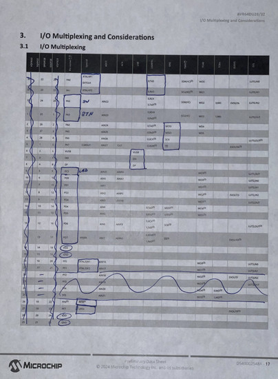
Personally, I like to start out with some high-level sketching on paper. Minimally, I want to understand the high-level block design of the solution and make note of key design considerations. I do this as I make a fast first pass through the data sheet. As part of this, I will compare with reference designs, if available. My first pass looks like this:
Using EasyEDA Pro
RX/TX Jumpers
A quick note on the serial RX/TX jumpers that I included. I wasn't very clear in the video about why I did this. I added these so that I can swap RX and TX signals. This shouldn't be needed; just make sure you connect the correct signals. :) I seem to get them swapped in some projects, so it's just a safety measure for me. I suppose it does also give me the capability to use standard serial cables or null modem cables by changing the jumpers (as null modem cables have RX/TX swapped on one end).
Corrections
I noticed the user button and reset button in the schematic were rotated 90 degrees from what I had in my mind. They should look like that in the image below. I will need to rotate the switches when I assemble the PCB (which won't be quite perfect).

Completed PCB (version 0.01)

Board Assembly & Testing
Related Content
I have uploaded the EasyEDA Pro source project and schematic PDF to my GitHub. See microcontollers/Microchip AVR64DU28 at main · rehsd/microcontollers
Walkthrough: Building a Small PCB in EasyEDA Pro (BGA CPLD Dev Board)
More to come!


Comments